
The research team led by Professor Der-Hsien Lien from the Institute of Electronics at NYCU recently collaborated with TSMC to successfully overcome the technical challenges of threshold voltage (VT) modulation in ultra-thin semiconductor layers. Their latest groundbreaking research introduced a photo-thermal method, integrating ultraviolet irradiation and oxygen annealing techniques, leading to an innovative direction in integrated circuit technology.
In recent years, research on two-dimensional and quasi-two-dimensional thickness semiconductors has been monumental as the miniaturization of semiconductor components develops. However, it has always been challenging to adjust the threshold voltage by altering the material carrier concentration in ultra-thin transistors since the dimensions of the materials are approaching or even smaller than the size of dopant atoms, making electronic transport and control extremely difficult. Therefore, achieving practical threshold voltage tuning has become a daunting challenge.
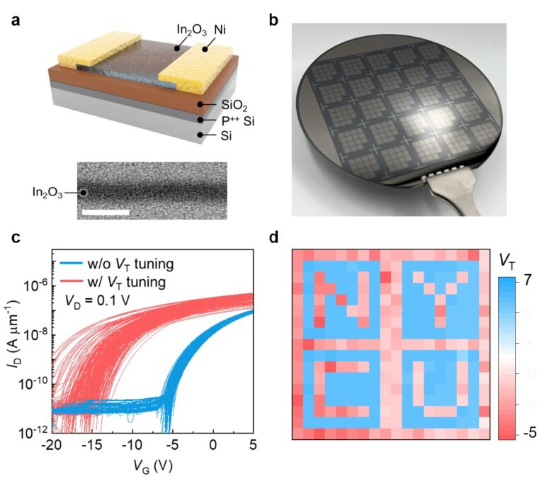
In this study, the research team introduced a photo-thermal method, combining ultraviolet irradiation and oxygen annealing, to achieve extensive and large-area VT modulation in ultra-thin indium oxide (In2O3) transistors. This method allows for both positive and negative threshold voltage adjustments and is reversible. The research team successfully demonstrated depletion-load inverters and multi-step logic by controlling VT, showcasing its potential in low-power circuit design and non-von Neumann computing applications. They also highlighted the practical applicability of this method beyond testing through wafer-size threshold voltage modulation using an automated laser system (in collaboration with RAEJA Technology).
The findings of this significant research achievement have been published in the internationally renowned academic journal Nature Communications, providing an essential direction for developing next-generation integrated circuit technology.
Related links: