The Hon Hai Research Institute (HHRI), in collaboration with the Institute of Electronics at National Yang Ming Chiao Tung University (NYCU), has made significant advancements in fourth-generation compound semiconductor technology. The joint research team has enhanced the high-voltage tolerance of fourth-generation Gallium Oxide (Ga2O3) semiconductors, opening up new possibilities for high-power electronic components in high-voltage and high-temperature applications. The research findings have been published in the highly influential materials science journal Materials Today Advances (MATER TODAY ADV).
Ga2O3: The Next Generation of Semiconductors Revolutionizing High-Power Applications
Gallium Oxide (Ga2O3), a fourth-generation semiconductor, is considered a leading candidate for next-generation semiconductor materials due to its exceptional properties. It features an ultra-wide bandgap of 4.8 eV and a very high critical breakdown field strength of 8 MV/cm, giving it significant advantages over existing materials like silicon (Si), silicon carbide (SiC), and gallium nitride (GaN). These characteristics make Ga2O3 suitable for high-power applications, such as electric vehicles, power grid systems, and aerospace industries.
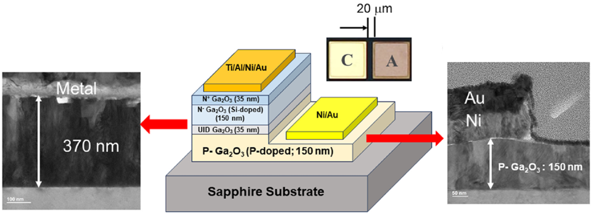
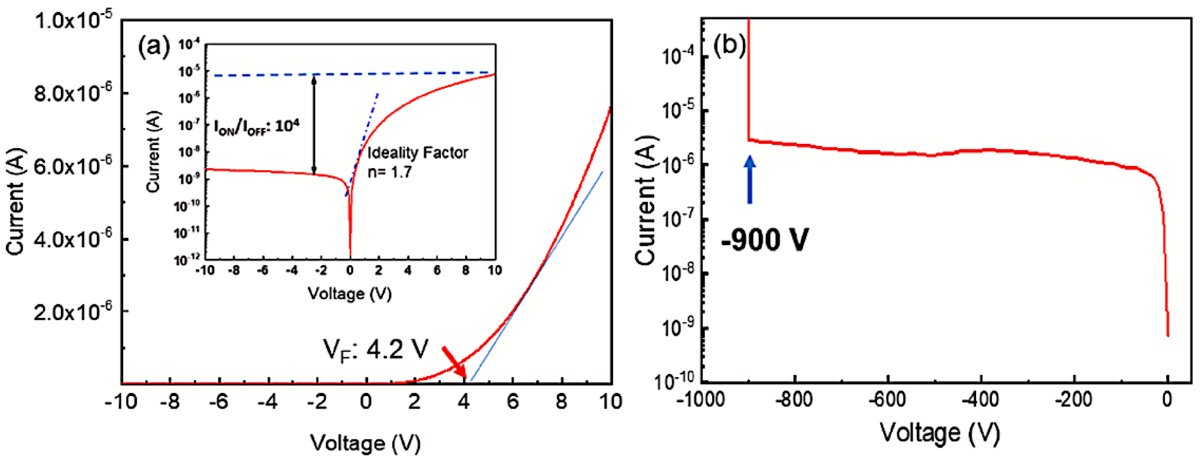
The research titled “Heteroepitaxially Grown Homojunction Gallium Oxide PN Diodes Using Ion Implantation Technologies” was conducted by Dr. Hao-Chung Kuo, Director of the Semiconductor Research Center at HHRI and Chair Professor at NYCU, along with his team at the Semiconductor Research Center, in collaboration with Professor Ray-Hua Horng’s team from the Institute of Electronics at NYCU. The team utilized phosphorus ion implantation and rapid thermal annealing techniques to achieve the fabrication of P-type Ga2O3, a fourth-generation semiconductor. They then regrew N- type, and N+ type Ga2O3 onto it to form PN Ga2O3 diodes, demonstrating excellent electrical performance. This breakthrough technology significantly enhances the components’ stability and reliability and reduces electrical resistance.
This research has been published in the high-impact international materials science journal Materials Today Advances. In 2023, Materials Today Advances had an impact factor of 10.25 and ranked in the top 25% of the Scimago Journal & Country Rank (SJR) in the materials science field. The journal has become an important platform for promoting the dissemination of knowledge and academic exchange among scientists and engineers worldwide.
Ga2O3 Set to Rival SiC in Power Electronics: Paving the Way for Broader High-Performance Applications
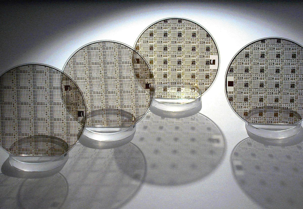
The Hon Hai Research Institute believes that Ga2O3 components have the potential to become competitive power electronic devices capable of directly competing with SiC components. China, Japan, and the United States are leading in Ga2O3 research. In particular, Japan has industrialized 4-inch and 6-inch Ga2O3 wafers, while several research institutions and companies in China are actively advancing related research and product development.
As Ga2O3 technology develops, broader applications in high-voltage, high-temperature, and high-frequency fields are expected to be found. We will continue to dedicate ourselves to research in this area, contributing to global technological innovation and industrial advancement.